 Engineer News Network The ultimate online news and information resource for today’s engineer
Jochen Kern explores best practices for designing with photo-chemical etching (PCE), highlighting how the process not only supports but actively stimulates new thinking in product development
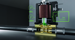
In high-tech manufacturing, success is increasingly measured not just by what is made, but by how it is made. Miniaturisation, integration, and performance pressures are forcing engineers to rethink traditional production methods. Among these, photo-chemical etching (PCE) has emerged as a critical enabler of next-generation metal components, capable of delivering ultra-fine features, tight tolerances, and burr-free parts without the mechanical or thermal stresses of traditional processes.
Yet, as with any manufacturing method, getting the best out of PCE is not automatic. It requires an understanding of how to design specifically for the process, a discipline we call Design for Photo-Chemical Etching (DfPCE). When engineers embrace DfPCE principles early, they can unlock extraordinary precision, cost efficiency, and innovation potential.
This article explores best practices for designing with PCE, highlighting how the process not only supports but actively stimulates new thinking in product development.
One of the most common missteps engineers make is treating PCE as a direct substitute for stamping, punching, or laser cutting. While PCE can replicate those results, its true value emerges when designs go beyond what those processes can achieve.
Unlike mechanical or thermal cutting, PCE creates complex geometries with no tooling wear, no deformation, and no burrs. This enables patterns, apertures, and profiles that would be impractical or impossible with traditional methods.
Best practice. When designing for PCE, do not simply copy existing stamped or laser-cut designs. Start with a blank sheet. Ask: “If constraints of tooling and heat stress disappear, what new functionality could this component deliver?” This shift often leads to breakthrough designs with improved performance and lower overall system cost.
The importance of tolerancing
PCE’s defining feature is its ability to maintain exceptionally tight tolerances across thin metal parts. But tolerancing decisions made during design have a direct impact on both precision and cost.
Because PCE is mask-based, every feature on a part can be controlled photolithographically, allowing for consistency across thousands (or millions) of pieces. Yet, designers sometimes specify tolerances tighter than necessary ‘just in case’, which can drive up cost or limit scalability.
Best practice. Define tolerances functionally. If a feature’s performance window is ±10 microns, there’s no need to specify ±5. Work collaboratively with your PCE supplier early in the design phase to determine realistic tolerances that balance performance with manufacturability.
Matching alloys to application
PCE can process a wide range of metals and alloys, stainless steels, nickel-iron, copper, titanium, beryllium copper, and more. Each material responds slightly differently to the etching process, influencing achievable precision, edge quality, and cost.
Often, OEMs approach PCE suppliers with a ‘must-use’ material already in mind. But in many cases, an alternative alloy (still meeting performance requirements) may etch more cleanly, hold tighter tolerances, or deliver better cost efficiency.
Best practice. Involve your PCE partner at the material-selection stage. Discuss the functional requirements first (conductivity, strength, corrosion resistance) rather than prescribing an alloy. Suppliers with broad experience can recommend the optimal material and thickness for both performance and processability.
Etching profiles and crosscections
One of the least discussed aspects of PCE is its ability to produce asymmetrical or profiled cross sections. With proprietary mask and exposure control, it is possible to create tapered slots, chamfered edges, or multi-level features directly in the etch, without secondary machining.
This capability is particularly valuable in applications like microfluidics, EMI shielding, or precision filters, where flow characteristics or electrical performance depend on the geometry of the aperture itself.
Best practice. Work with your PCE supplier to explore multi-level etching or controlled profile shaping. Many engineers are surprised to discover that features they assumed would require secondary machining can be produced directly, saving cost and time.
Designing for prototype-to-production consistency
Another overlooked strength of PCE is its scalability. Because the process uses digital photo-tools rather than hard dies, moving from prototype to full production is fast, cost-effective, and consistent.
However, scalability still requires forethought. For instance, a part designed for prototype batch etching may need slight modifications to take full advantage of high-volume reel-to-reel processing.
Best practice. Design with the production method in mind from the start. Ask your supplier how a part would transition from sheet-fed prototyping to reel-to-reel production. This ensures the same design can be manufactured at scale without costly redesigns.
Minimising post-processing
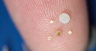
Mechanical cutting almost always produces burrs, which can compromise assembly, safety, and performance. Removing burrs adds cost, time, and sometimes risk. PCE, by contrast, produces burr-free parts directly from the process.
This advantage multiplies in industries like medical devices or semiconductors, where clean edges and material integrity are essential. For example, a burr on a microfluidic channel can change flow rates. A burr on an implantable device can compromise biocompatibility.
Best practice. Consider where PCEs burr-free nature can eliminate secondary processes or open up new product architectures. For instance, ultra-fine apertures can be created without risk of blockage or deformation, enabling new classes of filters, meshes, and shielding components.
Design partner
The greatest gains in PCE come when OEMs treat their supplier as a design partner rather than a part producer. Early collaboration allows for optimisation of geometry, material, and tolerances, reducing iteration cycles and avoiding costly last-minute changes.
At the Micro Component Group, for example, we routinely work with customers from concept stage through prototyping and into high-volume production, ensuring designs are optimised not just for performance but for manufacturability and scalability.
Best practice. Involve your PCE supplier at the earliest possible stage of product development. Share functional goals, constraints, and priorities. This collaborative approach often reveals opportunities for cost reduction, performance improvement, and faster time-to-market.
Designing for PCE is not just about cost or precision, it is about unlocking new innovation pathways. Because the process imposes so few constraints, it encourages creative thinking and rapid iteration.
In fields like EV battery technology, for example, PCE allows for intricate current collector patterns and lightweight busbars that improve efficiency without sacrificing reliability. In medical devices, it enables features so fine they blend seamlessly with polymer microstructures. In aerospace, it produces lightweight, high-strength components that meet strict environmental and performance standards.
In each of these cases, the technology did not just meet a need, it inspired new solutions. This is the real power of DfPCE, using the process not merely as a manufacturing step but as a design enabler.
As industries push toward smaller, smarter, and more integrated systems, PCE will play an ever-greater role in enabling precision metal parts. But to fully harness its potential, engineers must embrace a mindset of designing for the process.
The key principles are straightforward:
- Start with PCE’s capabilities, not traditional constraints.
- Define tolerances functionally, not habitually.
- Involve your supplier early in material and process decisions.
- Explore multi-level etching to eliminate secondary machining.
- Plan for scalability from prototype to production.
These practices transform PCE from a manufacturing method into a platform for innovation, one that delivers measurable advantages in cost, performance, and time-to-market.
Final thoughts
I have seen first-hand how embracing Design for PCE reshapes what is possible in metal component manufacturing. This is no longer a niche process for specialty parts, it is a mainstream technology driving the next wave of product innovation.
In a world where every micron counts, precision is not just a requirement, it is a competitive advantage. By designing for PCE from the start, OEMs can achieve that advantage, opening up opportunities to rethink products, streamline production, and deliver value in entirely new ways.
If your team has never explored what PCE can truly offer, now is the time to start.
Jochen Kern is Head of Sales & Marketing, Micro Component Group.