 Engineer News Network The ultimate online news and information resource for today’s engineer
Photo chemical etching is the go to process for the manufacture of precision metal parts and components. Jochen Kern highlights the process advantages of the technology and explains why photo etching is used in a growing number of exacting industrial applications
Photo Chemical Etching (PCE) is today respected as a precise manufacturing process used to fabricate intricate metal components. It involves the use of chemical and photographic techniques to selectively remove material from a metal sheet, resulting in the desired design.
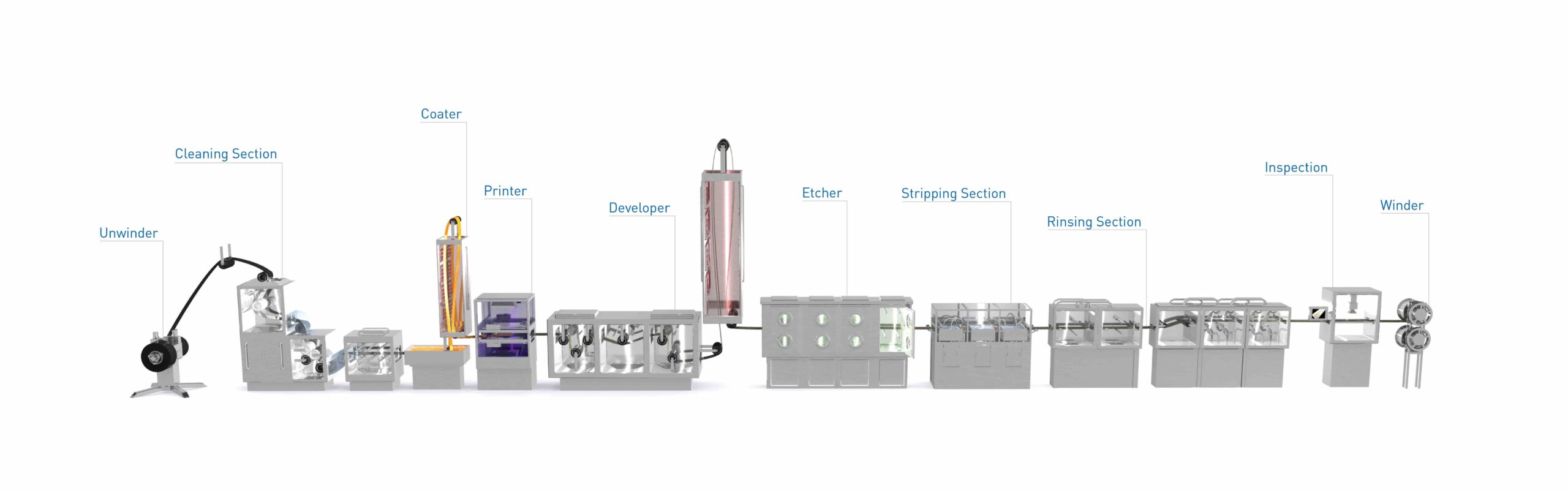
The process begins with cleaning the metal sheet to remove oils and contaminants. A photo tool, typically a high-resolution glass, film, or digital image, is applied to the laminated metal sheet. UV light is used to expose the design onto the film, which transfers it onto the metal surface.
After the exposure, a development solution is applied to selectively remove the excess resist from the unprotected areas, leaving behind the desired part design. The metal sheet is then subjected to an etching process, where a chemical solution is applied to dissolve the unprotected areas of the metal. This results in the precise removal of material according to the design, leaving behind the desired component.
Once the etching process is complete, the finished part is immersed in a stripping solution to remove any remaining resist and contaminants. The etched parts are then ready for further processing, such as bending, assembly, or final quality control inspections.
Process advantages
PCE is a sophisticated manufacturing process that offers significant advantages over traditional metal fabrication methods. It enables the production of complex designs with exceptional precision and tight tolerances, making it suitable for a wide range of applications.
One of the key advantages of PCE is its ability to preserve the physical properties of the metal being etched. Unlike traditional mechanical fabrication methods, such as stamping or machining, PCE does not subject the metal to excessive mechanical forces or heat. This means that the inherent properties of the metal, such as hardness, ductility, and grain structure, remain largely unaffected. Consequently, the final etched components retain their original mechanical characteristics, ensuring optimal performance and functionality.
The process is also highly cost-effective, particularly when it comes to tooling costs. PCE utilises digital tooling to transfer the image onto the metal surface. The cost of producing an engineered tool for PCE is relatively low, typically around €2000. In comparison, traditional metal fabrication methods often involve expensive and time-consuming tooling processes, which can cost several thousand dollars and require significant lead times. This cost advantage makes PCE particularly attractive for small to medium-scale production runs, as well as for rapid prototyping.
Furthermore, PCE allows for quick and easy design changes during the prototyping stage. Since the tooling process is relatively straightforward and affordable, modifications to the design can be implemented with minimal cost and time investment. Designers and engineers have the flexibility to make adjustments to the dimensions or features of the part, ensuring that the final product meets the desired specifications.
Another notable advantage of PCE is its ability to produce burr-free parts with smooth edges. The process removes material through chemical dissolution, resulting in clean and precise edges without the formation of burrs or rough areas. This level of precision is especially crucial for applications that require intricate details, such as fine screens, circuit components, or medical devices, where any imperfections or burrs could compromise performance or safety.
Additionally, PCE is compatible with a wide range of metals and alloys. Stainless steel alloys, steel alloys, brass, copper, beryllium copper, aluminum, Inconel, nickel silver, phosphor bronze, and various exotic alloys can all be successfully etched using this process. This versatility enables the production of components for diverse industries, ranging from electronics and aerospace to medical equipment and telecommunications.
Next generation PCE
The micrometal Etching Group has evolved the already precise PCE technology, and has optimised the process so that today it offers levels of precision and tolerance attainment impossible using traditional PCE or any other more traditional technologies.
There are many stages in the PCE process, and micrometal has focused in on a couple in particular to refine the technology to cater for the ever more exacting requirements of customers throughout industry. micrometal’s PCE process is very different from conventional PCE processes. The company uses a special liquid resist system to obtain ultra-thin (2-8 micron) photoresist layers enabling a higher degree of precision in the chemical etching process. It allows the achievement of extremely small feature sizes of 25 microns, a minimum hole diameter 80% of the material thickness, and single-digit micron tolerances repeatably. In addition, along with the company’s optimised exposure system it can avoid the parallax problems typically associated with PCE.
Traditional PCE uses relatively thick dry film resist which compromises ultimate part precision and the tolerances that are available, and it is only able to achieve 100-micron feature sizes and a minimum hole diameter of 100-200% material thickness. The micrometal Etching Group PCE process enables ultra-precise contours to take shape, and as such the company can produce metal parts with unique features and a level of complexity that cannot be matched. Because of this micrometal considers its PCE process to be an enabling technology, producing hitherto impossible metal parts and components, and therefore driving industrial innovation for customers.
The micrometal Etching Group PCE process enables ultra-precise contours to take shape, and as such the company can produce metal parts with unique features
In addition to our use of wet resist instead of dry resist, whereas most PCE service suppliers use digital photo tooling created on films, micrometal uses photo tooling created on glass, which caters for the many applications that require extreme precision. Glass photo tooling can achieve tolerances in the range of 1-2 microns, and negates issues with distortion due to environmental factors such as humidity that are a constant problem when using film tooling. By way of example, over a 700 mm etch area, micrometal can consistently achieve 5-10 micron tolerances, whereas PCE companies using film-based tooling can only claim 50-60 micro tolerances.
PCE from micrometal has many attributes that can truly stimulate innovation and stretch the boundaries of what is perceived as possible with the inclusion of challenging product features, enhancements, complexity, and efficiency, and it is important that design engineers fully exploit its potential. Optimum success involves early-stage engagement with a PCE specialist. A partnership needs to be forged, not a customer/subcontractor relationship if the true potential of micrometal’s PCE is to be realised, and so the company invites customers to present applications for review to discuss how PCE can help in product development programs.
Summary
Traditional PCE is a versatile and efficient manufacturing technique used in industries that demand high-quality, intricate metal components. Its applications span across electronics, aerospace, medical equipment, telecommunications, automotive, and more. The process’s ability to achieve precise designs, tight tolerances, and its compatibility with various metals make it an essential solution for industries seeking reliable and cost-effective manufacturing processes. micrometal’s next generation PCE technology pushes the boundaries of this already precise and agile technology, and is enabling innovation across an array of precision metal component manufacturing.
Jochen Kern is Head of Sales & Marketing, micrometal GmbH.