 Engineer News Network The ultimate online news and information resource for today’s engineer
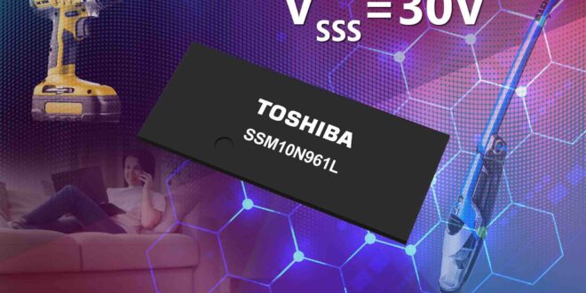
Toshiba has launched its first 30V N-channel common-drain MOSFET. The new SSM10N961L device offers low-loss operation and is specifically intended for use within devices with USB interfaces. Additionally, it may be used for protecting battery packs within mobile applications.
With the ubiquity of USB interfaces, many components and devices have been developed to support USB standards. The USB Power Delivery (USB PD) standard supports higher power levels from 15W (5V/3A) to a maximum of 240W (48V/5A) and allows swapping of the power supply and receiving side. This requires devices with USB charging to support bi-directional power and this is the use case that the new SSM10N961L N-channel common drain MOSFET has been designed for.
Until now, Toshiba’s N-channel common-drain MOSFETs have been 12V products primarily intended for the protection of lithium-ion (Li-ion) battery packs within smartphones. The newly released 30V product can be used for applications requiring voltages higher than 12V such as load switching for power lines of USB charging devices and the protection of Li-ion battery packs for battery-powered appliances.
The SSM10N961L combines two N-channels in a common drain configuration which is the feature that allows for bi-directional operation. The source-source breakdown voltage (V(BR)SSS) is 30V for use in higher voltage applications such as those found in laptops and tablets. To reduce losses in all applications, the source-source on-resistance (RSS(ON)) is typically 9.9mΩ.
When mounted on an 18µm, 407mm2 Cu pad, the current rating of the device is 9.0A. If the pad size and thickness are increased to 70µm and 687.5mm2, the current rating increases to 14.0A.
Despite the power handling capability of the SSM10N961L, the device is housed in a small thin package (TCSPAG-341501) measuring just 3.37mm×1.47mm x 0.11mm thereby allowing for high-density solutions to be developed.
By combining the new device with a TCK42xG driver IC it is possible to form a load-switching circuit with a backflow prevention function or a power multiplexer circuit that can switch operations between Make-Before-Break (MBB) and Break-Before-Make (BBM).