 Engineer News Network The ultimate online news and information resource for today’s engineer
Jochen Kern shows how the precision micro metal manufacturing process, photo-chemical etching, can help to maximise precision, yields, and cost efficiency
Designing for photo-chemical etching (PCE) is not just about making an existing metal part a bit thinner or a bit cheaper. Done well, it changes what the part is (how it functions, how it is assembled, how reliably it performs, and how economically it can be scaled from tens to millions).
Yet in many projects, PCE is still treated as an afterthought, a ‘manufacturing option’ evaluated once the drawing is frozen. That is a missed opportunity. The real value lies in designing with the process, not merely designing into it.
In this article I would like to explore some practical strategies for designing for PCE that maximise precision, yield, and cost-efficiency, and (equally importantly) expand the design space for medical and high-tech applications.
Think in 2.5D, not 3D machining
The first mindset shift is to stop thinking like a machinist.
PCE works on sheet or strip material, removing metal from both sides using patterned photoresist and controlled chemistry. You are essentially sculpting in 2.5D, ultra-precise through-features, profiles, and locally adjusted thicknesses all defined photolithographically.
That has consequences for design:
- Profiles are ‘free‘ – adding more intricate outlines or internal apertures rarely increases cost, as long as they respect design rules.
- Depth features need planning – half-etches, step structures, and functional surface textures are powerful tools, but must be balanced with etch factors (sidewall taper) and material thickness.
- Stack functions – with PCE you can create springs, filters, features for location, and current paths in a single part. Ask “which features can I combine into one etched plane?” rather than “which parts do I need to assemble?”
Teams that embrace this PCE way of thinking routinely cut part counts, reduce assembly steps, and improve reliability, because there is simply less to go wrong.
Design rules as enablers, not limitations
Every PCE process has design rules such as minimum web widths, hole diameters, distances between features, tolerances as a function of thickness, preferred corner radii, and so on.
These should not be treated as a restrictive checklist. Instead, they are the map of where you can safely push the process.
A good strategy is to start with the ‘comfort zone’, design critical features well inside the minimum values to maximise yield and robustness. Reserve the extremes for performance-critical areas where a very fine slot, tight gap or sharp edge truly provides differentiated product behaviour. Finally, use symmetry cleverly, symmetrical features etch more predictably, so avoid isolated ‘hero’ geometries in an otherwise sparse panel that will etch differently.
At Micro Component Group we often see two failure modes. The overly conservative design that misses PCE’s potential, and the ‘heroic’ design where every feature is right on the limit, eroding yield. The sweet spot is a deliberate mix, pragmatic where it doesn’t matter, ambitious where it does.
Precision starts with materials
Design for PCE is also design for material behaviour.
Because the process does not introduce mechanical stress or heat-affected zones, the starting strip or foil is the main determinant of flatness, spring performance, and long-term stability. That means designers should: specify material properties, not just alloys (hardness, temper, grain structure, surface condition, and thickness tolerance all influence results); align geometry with material function (for springs and flexures, for example, use PCE to define precise stress distribution rather than over-designing thickness); consider corrosion and biocompatibility early (particularly in medical and sensor applications where subsequent coatings or surface treatments may interact with the etched topography).
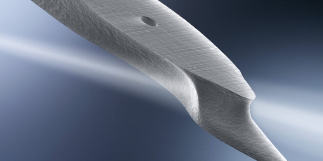
In practice, that often leads to counter-intuitive choices. Very hard, very thin materials that are difficult to stamp or grind become straightforward in PCE, enabling completely new needle, blade, or contact designs.
Panelisation and yield
When we talk about cost, we tend to focus on per-part price. In PCE, the economics are driven by area and panel utilisation.
A well-designed part that nests efficiently on a strip or sheet may be dramatically cheaper than a slightly smaller part that leaves unusable islands of metal. Designers rarely see this, but it is one of the most powerful cost levers.
Key strategies include:
- Design for tight nesting, use common radii and align features so parts tessellate with minimal scrap.
- Think about orientation, some geometries etch more consistently when aligned with the rolling direction; others benefit from rotation to balance etch behaviour.
- Plan for downstream handling, tabs, carrier frames, or reel-to-reel formats can improve throughput and reduce damage, boosting effective yield.
Early discussion between design and process engineers can turn an ‘expensive’ concept into a highly economical one simply by rethinking how it sits on the strip.
Tolerences
PCE can deliver tight and (more importantly) highly repeatable tolerances. But not every dimension needs to be microns-tight, and asking for that indiscriminately raises inspection effort and can mask what really drives function.
A more effective approach is to start from system behaviour, which dimensions influence sealing, flow, alignment, or cutting performance? Apply tight tolerances selectively, reserve the best capability for features that control those functions. And use functional datums, define reference features that reflect how the part is located and loaded in the assembly, not arbitrary edges.
Done well, this approach improves both yield and cost efficiency, while giving you a more robust, testable specification.
Pprotyping with purpose
Digital glass tooling and fast mask generation make PCE ideal for rapid iteration. The temptation is to treat this like a ‘try anything’ sandbox. That’s useful at first, but the biggest gains come when prototyping is used to learn about the interaction between design and process.
Good practice includes:
- Structured design of experiments – vary a few parameters at a time (slot width, bridge length, corner fillet, material temper) and measure performance, rather than changing everything between iterations.
- Capture process capability data – use early runs to understand real-world variation, not just nominal dimensions.
- Prototype under realistic conditions – especially in medical and environmental applications where fluid behaviour, tissue interaction, or thermal cycling dominate.
Each iteration then becomes an investment in knowledge, not just another sample.
Designing for assembly and the full value stream
PCE does not live in isolation. Parts need to be formed, coated, bonded, over-moulded, or assembled into larger systems.
Designing for PCE therefore means designing for the full value stream. Include forming requirements early (bend lines, local reliefs, and half-etched fold lines can be built into the artwork to control later forming precisely). Plan for coatings and joining (surface structures that promote adhesion, integration tabs, or local thickness variations can be etched in to improve robustness). Finally, always consider inspection and traceability (etched fiducials, codes, or identification features are virtually cost-neutral and strongly support quality systems).
When these conversations happen late, compromises are inevitable. When they happen at concept stage, they often unlock entirely new product architectures.
PCE as an innovation tool, not just a cost tool
Perhaps the most important shift is cultural.
Too often, PCE is brought in as a ‘plan B’ when other processes fail on cost or tolerance. In my experience, the most successful projects flip the script, they start with PCE because it expands what is possible.
In medical micro-needles, for example, designers have used PCE to create tip radii and multi-facet profiles that significantly reduce penetration force and patient discomfort. In sensors and actuators, ultra-fine, repeatable flexures and springs allow higher sensitivity and lower hysteresis. In battery and power electronics, intricate current paths and thermal spreaders can be tuned in ways stamping simply cannot achieve.
In each case, the design team did not just ask “can you make this drawing?” They asked “what geometry would your process like to make, and how can that improve our product?”
That is where precision, yield, and cost-efficiency align. When the part, the process, and the application are developed together.
Start the conversation earlier
Designing for PCE is not an esoteric art, it is a disciplined way of aligning geometry, material, process, and application. The strategies are straightforward:
- Think in 2.5D and stack functions into a single etched plane.
- Use design rules proactively to balance ambition and robustness.
- Choose and specify materials with the process in mind.
- Optimise panelisation for yield and cost.
- Apply tight tolerances where they truly matter.
- Prototype with intent and learn from each iteration.
- Design for assembly and the entire value stream.
As the Micro Component Group, we see our role increasingly as co-engineers rather than mere part suppliers. When we are involved early, PCE does more than fabricate metal, it reshapes products, compresses development cycles, and often makes previously ‘impossible’ ideas practical.
If you are exploring smaller, lighter, more complex metal components in medical or high-tech systems, the most important design decision you can make is simply this. Talk to your etching partner sooner. The rest follows from there.
Jochen Kern is Head of Sales & Marketing, Micro Component Group.