 Engineer News Network The ultimate online news and information resource for today’s engineer
In order to make microprocessors and memory chips more compact and to fit even more functionality into the smallest possible space, all production steps in semiconductor wafer manufacturing are subject to the most stringent requirements. This requires sensors that reliably monitor and control handling systems, machine parts, optics and other associated processes, says Glenn Wedgbrow
Semiconductor technology is the cornerstone of all modern technology. The progress of numerous industries depends on microprocessors and memory chips. The key drivers are smartphones, cloud computing and Big Data, plus megatrends such as artificial intelligence, the Internet of Things and autonomous driving.
At the same time, the requirements for semiconductor production are extremely high. Due to this, all sensors and systems need to be put through complex, rigorous manufacturing and testing processes. This includes the selection and placement of electronics, mechanical manufacturing, and special process technologies. In addition, special manufacturing processes and application-specific sensor materials must be used to meet the highest quality requirements. This enables individual sensor solutions to be manufactured that prove themselves in precision mechanical engineering due to high performance and precision, as well as robust design.
Measuring tasks in wafer production
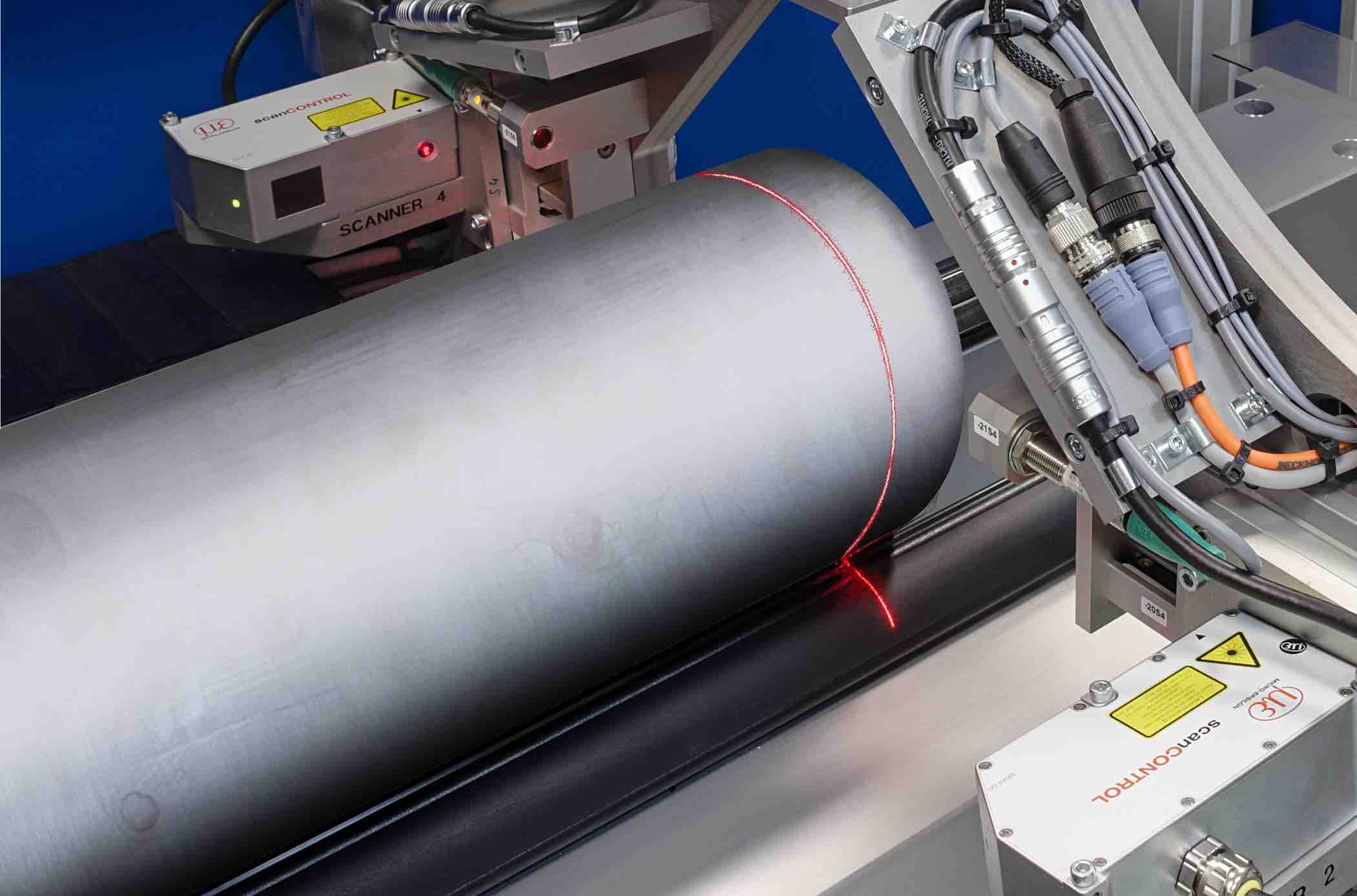
Ingot sawing requires high precision in processing. During sawing, the single crystal rod is cut into thin wafer slices using an internal hole saw. Wire saws, on the other hand, allow several slices to be cut from the bar at the same time. Non-contact sensors from Micro-Epsilon are used to monitor the sawing processes.
Dimensional inspection of silicon ingots
Initially, laser profile sensors measure the complete geometry of the silicon rod. To do this, the ingot passes a measuring station with several laser scanners. In a second step, the laser scanners check the dimensional accuracy of the orientation notches, which are later required for the exact alignment of the ingot. Blue laser scanners are used for this purpose, which generate a highly precise and interference-free measurement signal.
Monitoring the axial movement of internal hole saws
In the inner hole sawing process, wafers are sawn out of the silicon block. Here, eddy current sensors monitor the axial movement of the saw blades. As eddy current sensors are insensitive to dust and dirt, they provide precise measurement results even in adverse environmental conditions. The eddy current sensors measure the distance to the saw blade support without contact and so are wear-free. The result is a homogeneous and uniform cut of the silicon wafers.
Monitoring the deflection of wire saws
In wire sawing, several wafers can be cut from the silicon ingot simultaneously. The thin wires have a diameter of just over 100 µm. Due to abrasion, the wire wears out and loses about 5-10% of its diameter. Therefore, wire wear must be monitored continuously. Here, too, eddy current sensors are used, which record both the height of the wire and wire sag.
Colour measurement when cleaning wafers
For cleaning wafers, ozone is added to the cleaning liquid. Colour sensors from Micro-Epsilon are used to permanently determine the concentration of the contained ozone. These monitor the colour of the liquid and from this detect the ozone concentration. Even the smallest colour deviations of the concentration are reliably detected in the process.
3D shape measurement of wafers
The wafer slices created during sawing must be planar. Deflectometry systems from Micro-Epsilon record the flatness of the wafers with just one recording. 3D sensors project a striped pattern onto the wafer surface for this purpose. Integrated cameras record the reflected fringe pattern and the included software subsequently enables quick and easy evaluation. Distortions of the wafer would cause an equally distorted striped pattern. A highly accurate 3D representation enables the detection of such deviations at the micrometer level.
High-precision distance measurements in lithography
Photolithography is a central step in the wafer manufacturing process. In the exposure process, the image of a photomask is transferred to the wafer surface. A photosensitive photoresist layer was previously applied to the wafer. After stabilising this resist layer, the actual exposure begins.
Wafer lithography – especially EUV lithography – is one of the most complex industrial manufacturing processes. In order to deposit structures in the single-digit nanometer range on the wafer, the machine and optical elements must be positioned and aligned with correspondingly high precision. Sensors from Micro-Epsilon take on a decisive role here: nanometer-precise distance measurement in the positioning of the mask, the lens system and the wafer stages.
Positioning of the mask (reticle)
High resolution and long-term stable measurements of the machine movements must be made when feeding and positioning the lithography mask. Capacitive displacement sensors are used in this process to monitor mask alignment, meeting precision requirements in the nanometer range. The modular design with multiple sensor channels and the vacuum-compatible components enable use in numerous measurement tasks.
Confocal sensors are used to check the parallel alignment of the mask. The gap between the glass and the substrate is detected using just one sensor. The rectangular design of the sensors also allows installation in confined areas. In this version, the sensor requires only a minimum of installation space.
To achieve maximum measured value resolution, white light interferometers from Micro-Epsilon are used. These generate absolute readings with sub-nanometer accuracy and achieve accurate photomask alignment. Special evaluation algorithms and active temperature compensation ensure high signal stability. Similar to confocal sensors, the white-light interferometers are available in vacuum-compatible versions.
Alignment in the lens system
High-precision mirror optics are indispensable in lithography in order to achieve the highest possible imaging accuracy. To ensure that they function properly, the mirrors, lenses and lens carriers must be positioned precisely. In the same way, the horizontal and vertical movement of the individual optical elements must be monitored.
The alignment of the optics is measured using confocal chromatic sensors. This involves the nanometer-precise detection of the respective lens tilt. For use on glass, the confocal chromatic sensors and white light interferometers are the ideal choice.
The positioning of the lens carriers is monitored using capacitive displacement sensors. High precision capacitive sensors check the tilt to nanometer accuracy. Several sensors measure onto the metallic carrier, which ensures exact positioning and therefore reproducible light projection onto the wafer.
Non-contact eddy current sensors also measure the position of lens elements. Depending on the lens system, displacement sensors from Micro-Epsilon are used to detect movement and position in up to 6 degrees of freedom. Due to the high cut-off frequency, even highly dynamic movements of the lens systems can be monitored.
Position monitoring in the wafer stage
White light interferometers and eddy current sensors are used to monitor the position of the wafer stage or wafer platform. Here, they measure the XYZ movements of the stage, where extremely high accelerations occur. The high precision optical interferometers achieve sub-nanometer resolution and ensure that the wafer is optimally positioned for exposure. Vacuum-compatible measuring heads and insensitivity to strong magnetic fields enables the high precision sensors to be used in demanding environments.
Capacitive displacement sensors are used for fine positioning in the wafer stage. They measure the position of the stage at various points, which is necessary for fine alignment. Due to their triaxial design, the sensors are insensitive to electromagnetic fields and achieve a resolution in the nanometer range. In addition, they achieve extremely high long-term stability. The non-contact sensors are suitable for both vacuum and UHV.
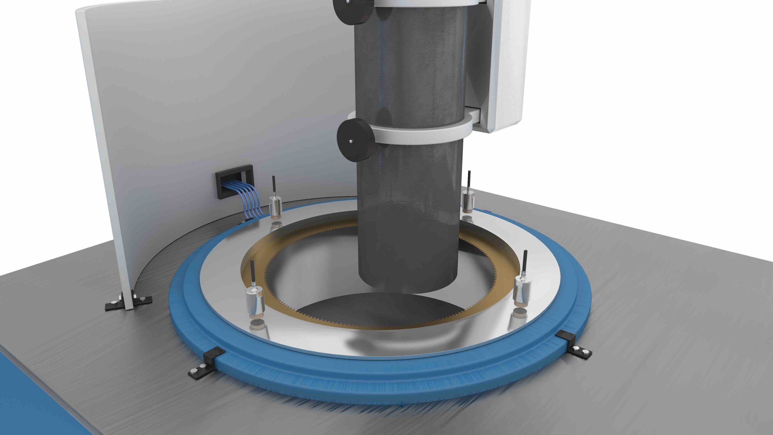
Inline wafer quality control
For quality control, sensors from Micro-Epsilon are used in various areas, for example, for testing the coating thickness, for monitoring the deflection, as well as separation. In addition to high precision, a high measurement rate is also required to support the high speed manufacturing processes.
Single-sided thickness measurement of transparent coating layers
Confocal chromatic sensors are used for one-sided thickness measurements of layers. The confocal measuring principle enables the evaluation of several signal peaks, allowing the thickness of transparent materials to be determined. Due to multi-peak measurement, even the thinnest layers are reliably detected. With just one sensor, the thickness of protective and paint layers, for example, are detected with micrometer precision.
Monitoring of wafer bow and warp
The larger the wafer, the greater the risk of deflection. Confocal chromatic sensors scan the wafer surface to detect bow, warp and distortion. With a measuring rate of 70 kHz, the confocalDT controllers enable highly dynamic measurements, which allows the wafers to be inspected in short cycle times.
Total thickness variation
Two confocal chromatic sensors measure the wafer thickness from both sides. The thickness profile of the entire wafer can also be used to determine the curvature and deflection of the wafer. High measuring rates enable thickness detection of the entire wafer in short cycle times.
Bumps
Confocal chromatic sensors from Micro-Epsilon measure precisely on shiny and textured wafer surfaces to determine the height of bumps with micrometer accuracy. Due to the focused light spot, a high lateral resolution of 4µm is achieved. In this measurement task, three sensors are moved above the wafer. From the three tracks, both the spherical shape and the height can be calculated precisely. This is possible because the controllers are connected via Ethernet and trigger input and so perform a synchronous measurement. In order to measure the high number of chips and therefore the bumps in the shortest possible time, Micro-Epsilon sensors offer an extremely high measuring rate of 70kHz.
Checking the saw marks, cracks and break-offs
Confocal chromatic sensors from Micro-Epsilon are used to detect cracks, saw marks and other defects on the wafer. They reliably detect surfaces with varying reflection characteristics due to a high speed surface compensation feature. An extremely small light spot and high resolution enable the reliable detection of the finest of anomalies on the wafer. The confocal sensors ensure reliable detection of the saw marks and other depressions in the wafer.
Highly integrated actuator systems for demanding environmental conditions
The Fast Steering Mirror from Micro-Epsilon is equipped with optimised non-contact displacement sensors. This micro-mechatronic actuator system is used for applications in the semiconductor industry to monitor the rapid tilting of the mirror, for example, in beam stabilisation and laser dicing.
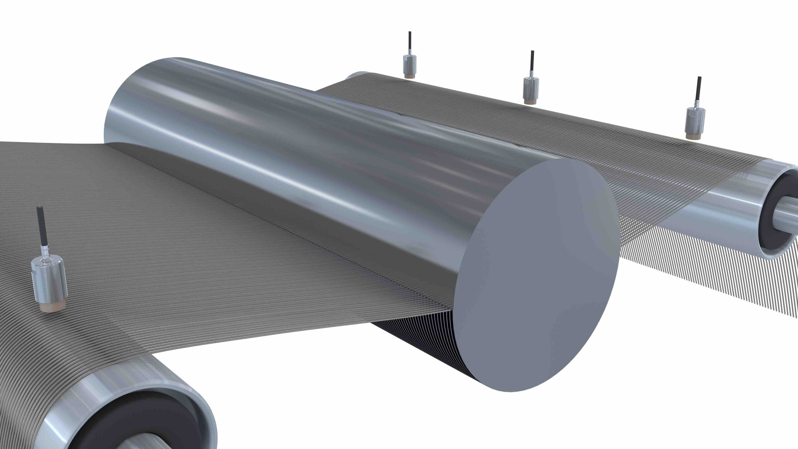
Precise monitoring in wafer handling
Wafers must be automatically removed and fed to the appropriate processing step throughout the manufacturing process. Accurate positioning is just as important as fast, reliable movement. Sensors from Micro-Epsilon ensure exact alignment and safe transport in every process step. The clean room suitability of the wear-free sensors is a basic requirement for their use.
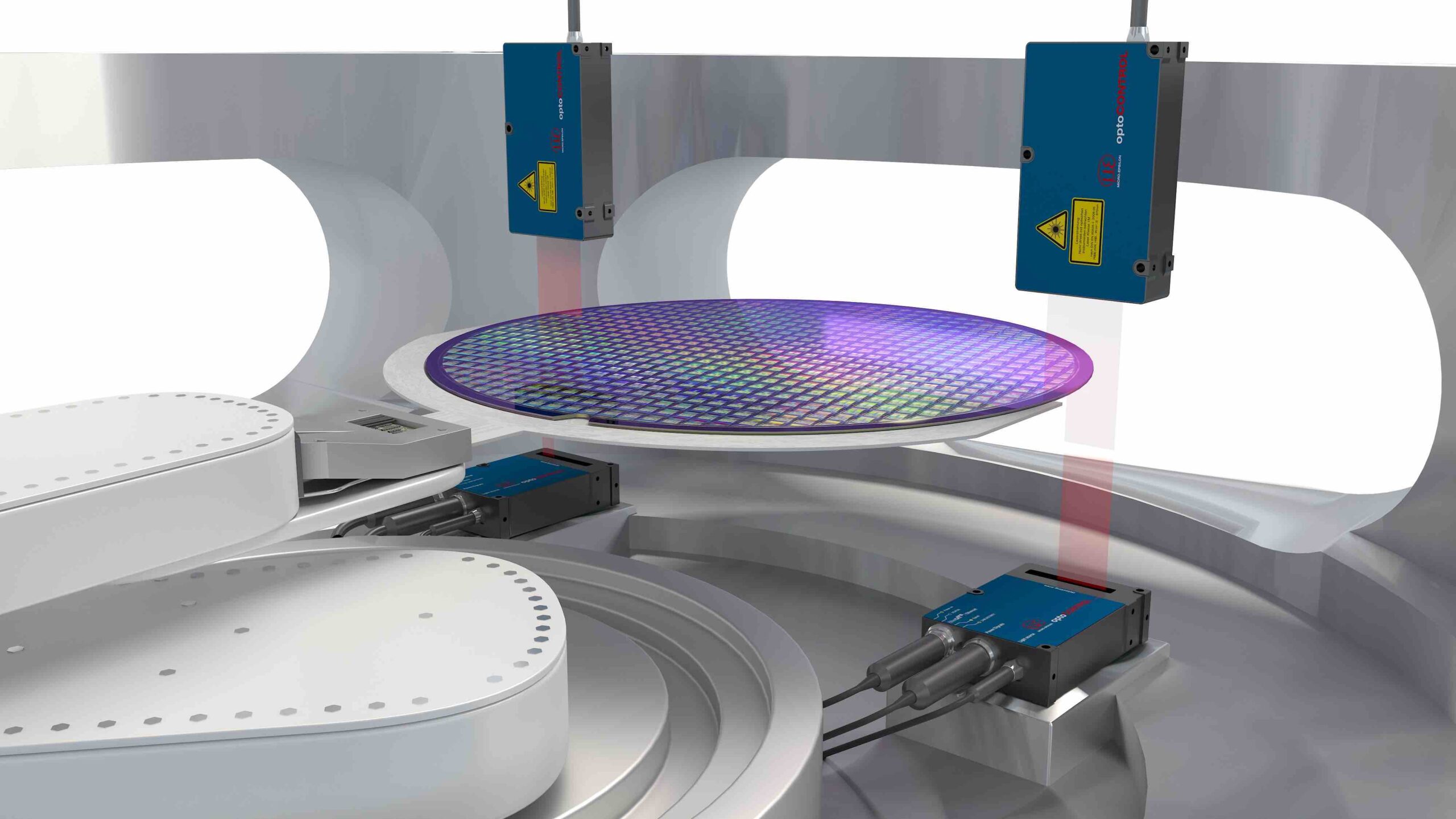
Precise edge detection of wafers using laser micrometers
Determining the position during wafer handling
When handling wafers, exact and repeatable positioning is crucial. During the infeed of wafers, two optoCONTROL laser micrometers inspect the diameter and thus determine the horizontal position. Due to the high measuring rate and accuracy, these micrometers provide reliable position information.
Tilt angle measurement of wafers
When feeding wafers, white light interferometers are used to measure their horizontal tilt. The interferometers provide absolute distance values at nanometer resolution. The measurement ensures the greatest possible positional accuracy when picking up and removing wafers.
Glenn Wedgbrow is Business Development Manager at Micro-Epsilon UK.