 Engineer News Network The ultimate online news and information resource for today’s engineer
In an era defined by smarter, faster, and smaller electronic devices, precision and scalability in metal part manufacturing are no longer competitive advantages, they are prerequisites for innovation.
From consumer wearables and implantable medical devices to advanced sensor arrays and next-gen communication modules, electronics miniaturisation is now the beating heart of product development. But miniaturisation is not simply a matter of shrinking designs, it demands new approaches to metal fabrication that traditional manufacturing methods often struggle to meet.
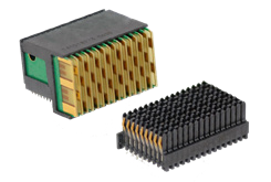
This is where photo-chemical etching (PCE), especially when delivered at scale and precision, changes the equation entirely.
Photo-chemical etching, according to the Micro Component Group, offers clear, intrinsic advantages over traditional machining, stamping, or laser-cutting techniques. For electronics OEMs and designers, the benefits are transformative:
- Stress-free processing: PCE removes material chemically, which introduces no mechanical or thermal stress to delicate features.
- Design freedom: PCE supports complexity at no extra cost, multiple geometries, intricate cutouts, and mesh-like patterns can all be fabricated from a single sheet.
- Ultra-fine tolerances: Achieving tolerances as tight as ±10 µm, PCE enables repeatable accuracy even for the most miniaturised circuits and components.
- Scalable to any volume: From early prototyping with fast lead times to full-scale reel-to-reel production in the millions, PCE scales with your product lifecycle.
- Material versatility: Whether stainless steel, copper alloys, titanium, or even molybdenum, PCE processes them all cleanly and efficiently.