 Engineer News Network The ultimate online news and information resource for today’s engineer
Photo-chemical etching (PCE) is a versatile and sophisticated metal machining technology, with an ability to mass manufacture complex and feature-rich metal parts and components. Dr. Angel Lopez discusses 10 considerations design engineers need to bear in mind when working with PCE
Photo-chemical etching (PCE) is a versatile and sophisticated metal machining technology, with the ability to mass manufacture complex and feature-rich metal parts and components. The process uses photo-resist and etchants to chemically machine selected areas accurately, and is characterised by retention of material properties, burr-free and stress-free parts with clean profiles, and no heat-affected zones.
Q. What do you consider to be the key attributes of PCE?
PCE is a technology that manufactures extremely complex metal components with no burrs and no stress-related issues that are common in other metal manufacturing technologies. This is down to the nature of the process which selectively removes material through chemical etching rather than mechanical stamping or high-temperature laser cutting, etc. It is also extraordinary in that it works through the use of inexpensive and easily designed digital or glass tooling, meaning no costly steel tool cutting, no long tooling lead times, and agility and versatility in the tooling process that allows for design tweaks and new iterations at next to no cost.
However, when it comes to design engineers and how they adapt their work to get the most from PCE, it is the boundaries that the process pushes that are of key importance. It is fair to say that for many applications, PCE is the only technology that can achieve the fine detail and repeatability that is increasingly demanded by OEMs in all industry sectors, and as such it can be said that PCE stimulates product innovation. A great place for any technology to be!
Q. What do design engineers need to know about the materials that PCE can be used with?
PCE can be applied to a vast array of metals of different grades, tempers, and widths in thicknesses from 0.01 – 0.4mm for reel-to-reel etching and up to 2mm thick for sheet etching. micrometal can supply specialist materials to customer demand on a case-by-case basis. Metals include steel and stainless steels, nickel and nickel alloys, copper and copper alloys, aluminium and hard-to-machine metals, including highly corrosive-resistant materials such as titanium and its alloys.
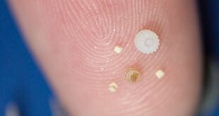
Q. What can PCE achieve when making small metal components?
Many applications require that precision metal components have specific characteristics which can include: ultra-high precision; very thin material; unique physical features; unique surface textures; identification features; extreme consistency part-to-part; ease of integration into the final device; and competitive cost. It is often a significant challenge to balance the combination of these characteristics while still maintaining cost and achieving production volume requirements. micrometal has consistently overcome these challenges through use of innovative techniques (see below), comprehensive design capabilities, and the world’s largest commercial reel-to-reel etch line. The reel-to-reel production process is characterised by excellent reproducibility and the attainment of very tight tolerances, producing the finest structures and contours out of the thin metal sheet. This etching process, therefore, guarantees individual customer solutions on an industrial scale.
The metal strips, which can be up to 800 meters long on spools, are particularly popular in industries that already have a high degree of automation in further processing. For example, the etched parts can be selectively coated, or used by ‘pick & place’ at the final point of use, processes that are popular in the medical technology and automotive industries.
With additional marking, numbering, or coding, etched products can be processed further in a trouble-free and automated manner.
Q. What tolerances can be achieved?
micrometal’s variation of the PCE process involves the use of very thin proprietary liquid photoresist (2-8 microns thick) and high-resolution glass photomask tools. This combination provides extremely precise control of the etching process, enabling configurations, features and tolerances that cannot be achieved by other methods such as stamping, laser machining, or traditional PCE. 3-dimensional features can actually be etched into the thickness of the material itself, and dimensional tolerances as low as ±0.005mm can be achieved.
micrometal can achieve extremely small feature sizes of 25 microns, minimum hole diameter 80% of the material thickness, and single-digit micron tolerances repeatably. Traditional PCE uses relatively thick dry film resist which compromises ultimate part precision and the tolerances that are available, and it is only able to achieve the smallest feature size of 100 microns, and the smallest hole diameter is a factor of 1-2 when compared to material thickness.
Q. Can’t laser cutting deliver more exacting tolerances than this?
Yes and no. Laser cutting can get down to tolerances of 5% of metal thickness, but it is often limited to a feature size of 0.2mm. As laser cutting is a ‘single point’ processing technology, it will also be disproportionately expensive for more and more complex parts, and it cannot achieve the depth features needed for micro-fluidic devices. First and foremost you must remember when using PCE, increased complexity does not mean increased cost.
Q. We hear a lot about PCE eliminating burrs and stresses inherent in other processes. Why is this?
Well, think about stamping, which is probably the sheet metalworking technology that comes closest to being able to make production parts as exacting and intricate as those we can make with PCE. Stamping makes parts from metal by literally stamping it under extreme pressures, often over 100 tonnes of pressure with modern machines. This causes changes in the metal being processed, and burrs are common around the edges of the stamped metal. These burrs need to be removed, and this means costly and time-consuming post-processing operations. PCE is a subtractive process that removes metal atom by atom using chemical etchants, so there is no shearing or thermal change to the material, meaning no burrs and heat-affected zones. Simple.
Q. In any manufacturing process, the lead times for tooling, and the cost of tooling are of huge importance. Is this the case with PCE?
You are right, tooling for most metal machining technologies requires hard tool steel, which is expensive and time-consuming to produce. Here again, PCE has obvious advantages, and at micrometal, we use high-resolution glass photomask tools, inexpensive to make, and very easy to adapt.
The cost of glass tooling does not increase significantly with part complexity, which cannot of course be said for steel tools. In addition, glass tooling does not wear out, and also it does not impart distortion and stress onto the metal being processed, and produces parts that are completely flat. In many instances, via PCE a part will have been manufactured in volume before the tool-maker has even pushed the button on the fabrication of a steel tool which then may have a lead time of months before completion.
Q. Manufacturers these days are looking for efficiency, but also cost-effectiveness in manufacturing. How does PCE measure up in this respect?
Many OEMs select PCE purely based on its cost-effectiveness as a production or prototyping technology. I have mentioned that the process is agnostic to part complexity, but also consider that with PCE you pay by the sheet not by the part, so this means that components with different geometries can be processed at the same time from one set of digital or glass tooling. The ability to produce many different parts in one production run means that the costs savings are huge. Couple this with the fact that there is no need to expend on costly steel tooling, and the overall savings inherent in the system are clear.
Q. What is the key to success in working with PCE specialist?
This is a good question, and I would say first and foremost the PCE company you choose should be treated as a product development partner, not just a sub-contract facility to outsource manufacturing to. There are so many inherent advantages to the process, and aspects to it that can be used for the benefit of component manufacture, that engaging the PCE specialist early in the design stage really pays dividends. From this point on, however, the key is experience.
micrometal has been active in and pioneering the use of PCE for over a decade, and as such has developed a knowledge base and expertise that is unrivalled. We have talked about the fact that PCE can be used on a huge array of metals, but this is not the case for all PCE companies, and comes from years of research and development into different etchant chemistries, and process optimisation in general. Through this dedication, we can now process soft, hard, and brittle metals, and difficult materials such as aluminium. Proprietary processes have also been developed which means that we are one of the only companies in the world that can photo-chemically etch titanium.
Q. You mention that OEMs and design engineers should partner with their chosen PCE specialist. Give us an example of what such a relationship can offer for product development?
Let’s look at something that is a part of the PCE process that no-one without an intimate understanding of the technology such as micrometal would know. Inherent in the way that PCE works is that it creates an edge ‘cusp’ during the process. An awareness of this and micrometal’s ability to control this means that we can produce a range of profiles that can be used to enhance product characteristics. Without close consultation with your PCE ‘partner’ such possibilities would be lost, and sub-optimal products may be the result.
Dr Angel Lopez is Director of Business Development at micrometal GmbH.