 Engineer News Network The ultimate online news and information resource for today’s engineer
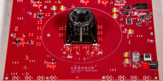
The Cadence test chip was fabricated in TSMC’s 7nm process and achieves a 4400 megatransfers per second (MT/sec) data rate, which is 37.5% faster than the fastest commercial DDR4 memory at 3200MT/sec.
With this key milestone, SoC providers developing high-speed memory subsystems for high-end server, storage and enterprise applications can start developing their DDR5 memory subsystems now with silicon-tested PHY and controller IP from Cadence.
“TSMC recognises the importance of next-generation DRAM for our enterprise and data center customers,” said Suk Lee, senior director of the Design Infrastructure Marketing Division at TSMC. “We’re pleased Cadence has proven interoperability with prototype DDR5 memory devices in our industry-leading 7nm process.
“This demonstrates a path to higher bandwidth and density for future server and storage devices manufactured at TSMC.”
“As part of Cadence’s DDR PHY validation and interoperability program, Micron has provided Cadence with engineering prototypes of the first memory for a preliminary version of the DDR5 standard,” said Ryan Baxter, director of Data Center segment, Compute and Networking Business Unit, at Micron. “We are enthusiastic that Cadence’s DDR5 IP test chip is able to interoperate consistently with our DDR5 prototype memory devices at the 4400MT/sec speed.”
“Cadence has taken a huge leap forward in enabling servers, storage and enterprise equipment with next-generation high-speed memory. Systems that use DDR5 will be able to achieve higher bandwidth than DDR4 while also using less power per bit transferred, enabling these systems to do more computing on larger data sets than what’s possible with DDR4,” said Babu Mandava, senior vice president and general manager, IP Group at Cadence. “Cadence next-generation DDR IP is ready for implementation now, and we look forward to enabling DDR5 SoC designs.”
Cadence[/highlight] is ready to engage with customers immediately to start SoC designs integrating DDR5 memory interfaces.